 The advent of the integrated circuit more than 50 years ago revolutionized the electronics industry, ushering in an era of rapid advancement in computing. In the intervening half century, we now have smartphones in our pockets that are more powerful than the earliest computers.
Since then, there has been a race to make these microchips smaller while achieving more computing power with lower costs and lower power dissipation. Intel co-founder Gordon Moore predicted early on that the number of transistors – the miniature electronic components that amplify or switch electric signals in microchips – would double on integrated circuits approximately every two years. Moore’s law, as it is known, has held true.
But engineers are beginning to reach the limit of how far they can scale down the transistors in integrated circuits with silicon technology, which has dominated the industry for so long. Researchers are exploring other materials and methods that may be better suited toward advancing micro and nanoscale electronics technology.
“We’re really reaching the end of the scaling predicted in Moore’s law,” said Mike Hamilton, director of the Alabama Micro/Nano Science and Technology Center at Auburn University and associate professor of electrical and computer engineering. “Researchers in the Alabama Micro/Nano Science and Technology Center are working to scale a little bit further, develop more efficient devices for computing systems and compute faster with less power. We’re also looking at new materials, devices and technologies altogether to be able to do something that’s parallel to that. That’s called More Than Moore or Beyond Moore technologies.”
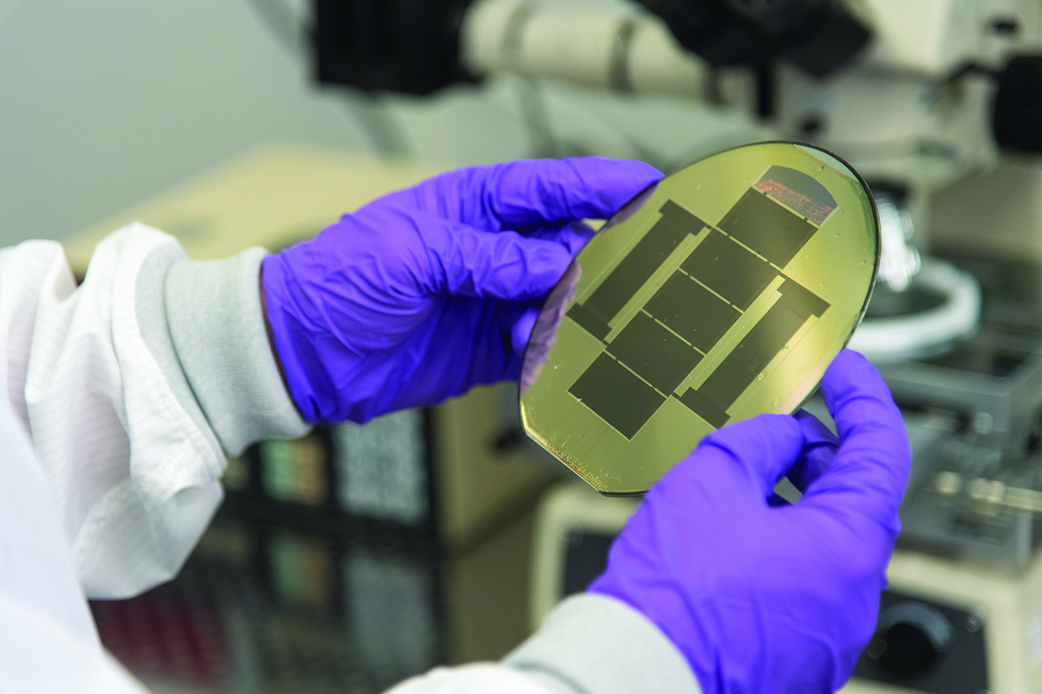
Since its establishment in 1984, the Alabama Micro/Nano Science and Technology Center has been at the forefront of research on microelectronics and nanotechnology. Its researchers have worked closely with government and industry over the years to address applied research in addition to the theoretical research it conducts.
With silicon-based technologies, engineers are able to scale down transistors to nanoscale dimensions. This year, electronic companies such as Samsung and Apple have begun using transistors in their products as small as 10 nanometers – multiple orders of magnitude smaller than a human hair. However, engineers can only scale down this technology so far.
“Eventually, we start to run into quantum mechanical effects where transistors just don’t function quite like they are supposed to,” said Mark Adams, assistant professor of electrical and computer engineering. “We’re certainly getting to that point.”
Researchers are looking beyond silicon to other types of materials to extend integrated circuits down to smaller and smaller geometries while achieving superior computing power.


Masoud Mahjouri-Samani, assistant professor of electrical and computer engineering, is one of the researchers exploring alternate materials for integrated circuits. Many engineered atomically-thin two-dimensional materials show great promise for the next generation of electronics with properties well-beyond conventional 3-D counterparts.
Mahjouri-Samani is working on a new class of atomically thin 2-D materials known as metal chalcogenides, which include tungsten ditelluride, molybdenum diselenide, gallium sulfide and others. The combination of these 2-D materials has the potential to create a new paradigm in next-generation transparent and flexible quantum electronics, photonics, optoelectronics and sensing devices.
The 2-D materials can be synthesized through processes such as chemical vapor deposition and metal organic chemical vapor deposition, but Mahjouri-Samani prefers using laser-based techniques to synthesize, process and make hybrid structures with these materials. He believes that the spatial, temporal and spectral tunability properties of lasers give him the power to control the synthesis processes more accurately.
“This is a big class of materials and only a few of them have been synthesized so far,” Mahjouri-Samani said. “They exist in a bulk form, but they do not exist in a single layer form, so to unleash their potential you have to synthesize them first. However, there are many challenges. For instance, how can we grow them as large as possible to make large-scale crystalline monolayers and how do we directly integrate them into different platforms?”
Aside from using different materials in integrated circuits, Auburn researchers are also exploring entirely different types of electronic systems for computing. Hamilton’s research group is studying superconducting electronics, as opposed to the traditional semiconducting silicon platforms.
“It’s a totally different method of storing and moving information, allowing us to evolve from something like a transistor to a device called a Josephson junction, and constructing integrated circuits based on superconducting devices,” Hamilton said. “You then get the advantages with superconducting circuits of having lossless elements, very low power dissipation and very high-speed operation.”
By utilizing new materials and superconducting circuits, researchers hope to open the door for quantum computing systems. Unlike classical computing systems, quantum computing can employ phenomena found in quantum physics, such as quantum superposition and quantum entanglement, to process information in new ways using quantum bits, or qubits. Once quantum computing systems are perfected, researchers believe they will be able to solve problems that classical computers never could.
“With quantum computing, we’re going to be able to make incredibly powerful computers that just put our classical computers to shame for certain types of computational problems,” Hamilton said.
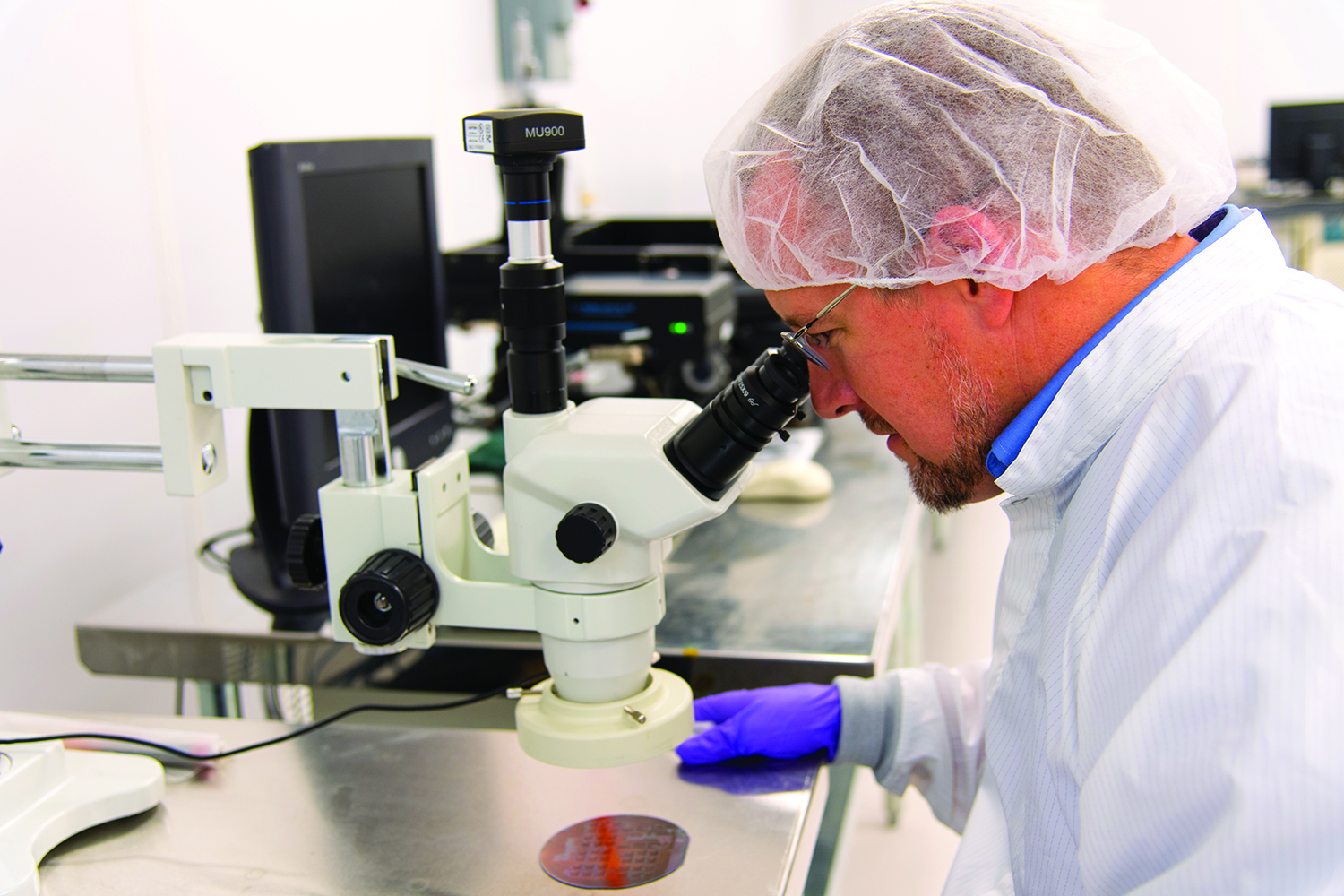
The Alabama Micro/Nano Science and Technology Center’s work goes far beyond finding new materials for integrated circuits and developing alternate computing architectures. In his Sensors, Transducers, Optics, Research and Modeling Laboratory, Adams conducts research in the area of fabrication, integration and packaging of microelectronic systems.
His research runs the gamut from ensuring an environmental sensor probe can operate at 50,000 feet to developing a contact lens with microelectromechanical systems, or MEMs, to diagnose traumatic brain injury.
“A lot of my work is solving usability problems,” Adams said. “We’re not necessarily building a chip that sits in a computer. We’re trying to build devices that are flexible and wearable, so there’s still a huge challenge on the usability side of that. There are also reliability challenges in getting a specific device to function at a really high g-force or really high temperatures. There’s a lot of engineering that has to be done in order to accommodate that.”
From developing the next generation of integrated circuits to the development of quantum computing and beyond, the Alabama Micro/Nano Science and Technology Center’s researchers are conducting leading research in these areas.
“I’m really proud to say that we have a large number of high-quality faculty here at Auburn working across these different areas whether they are in electrical and computer engineering, computer science, physics or another STEM-related department,” Hamilton said. “We have strong research groups, and our top-notch facilities and equipment are able to support pioneering research in microelectronics and nanotechnology.”