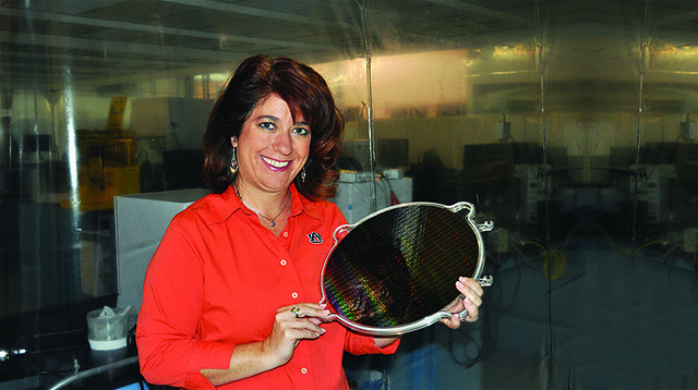
Diane Hickey-Davis, referred to by friends as “Dr. Diamond,” incorporates thin film diamond for global semiconductor companies. Pictured here in front of a Class 1000 clean room, she is holding a patterned diamond-on-silicon wafer designed for advanced computing. With a passion for conveying her love of engineering and science to others, she also leads demonstrations for Nanodays at Northwestern University and Sisters-for-Science, participates in robotics competitions and leads sessions at science camps with hands-on nanotechnology demonstrations for kids. In fact, she even met her husband, Mike Davis, a.k.a. “the science guy of Chicago,” at a NSF Nanotechnology Outreach Conference. Hickey-Davis says their 2-year-old son Giovanni is already exhibiting the signs of an engineer.
Diane Hickey-Davis
’96, chemical engineering
’04, M.S.,‘07 Ph.D., materials science and engineering, University of Florida
General manager, Semiconductor Business Unit
Advanced Diamond Technologies, Chicago
Early years . . . my father, brother, two uncles and grandfather are engineers – it’s in my blood; my mother worked for a scientific instrument company – I was the only 5-year-old who had “infrared spectrophotometer” in her vocabulary.
Typical day . . . I make, study and sell diamond, which is an amazing material – it has a very low coefficient of friction meaning it is slippery. Man-made diamonds, like those that are mined, are made of carbon. The material we make is a polycrystalline thin-film, which is many diamond crystals grown together from carbon in a gas, similar to the way that ice crystals form on a windshield using the water vapor in the air.
Current projects . . . working with a world-famous scientist to incorporate thin film diamond into a project for the renewable energy industry; coordinating testing for a thermal diamond product that could increase the heat transfer rate in electronic devices to increase efficiency; introducing a new product – an all-diamond probe – into the force microscopy industry.
My Auburn Engineering . . . taught me to estimate a reasonable answer range before I begin work on the solution, to be reasonable with my significant digits and include error in my answers. Almost daily, I ask for the thickness of a thin-film being produced with data taken using a profilometer and software – and read by a human. Any engineer knows that specs and tolerances are extremely important – so is being practical and reasonable.
Turning point . . . assisting with the development of a non-profit science education foundation and realizing how much I missed science. I wanted to know why glass is transparent, why metal feels cold to the touch, and how a computer works, so I pursued my master’s and then realized that grad school was just a big science camp! They paid me a stipend, and let me play on multi-million dollar microscopes and look at rows of atoms in man-made diamonds! How cool is that?
Geek moment . . . designing my own orange and blue class ring and choosing diamonds with visible defects because I studied defects – two blue diamonds . . . for every one million carbon atoms, there is one boron atom sitting in the lattice – and one orange diamond – for every 10,000 carbon atoms, there’s one nitrogen atom. Boron and nitrogen are “p” and “n” type dopants, making my ring a “p-n-p” junction. Engineers love it.
Sense of pride . . . the common thread that runs throughout my career started at Auburn – I helped initiate the Cupola Engineering Ambassadors with a mission to “promote, unify and serve the College of Engineering.” Those tenants have impacted every aspect of my life – promoting science and engineering, explaining the impact it has on our lives, and unifying people for common causes.
